Assembly Process
We work as your trusted partner to manage the entire PCB assembly process by coordinating with reliable manufacturers and service providers. From sourcing components and checking your PCB design to getting the boards fabricated and assembled, we handle everything through our expert network. Before production begins, we take care of important steps like finalizing the Bill of Materials (BOM), verifying the layout, and making sure all parts are ready. Our service saves you the time and effort of managing multiple vendors, reduces risks, and ensures smooth, high-quality results—from start to finish.
🔍 BOM Costing & Management
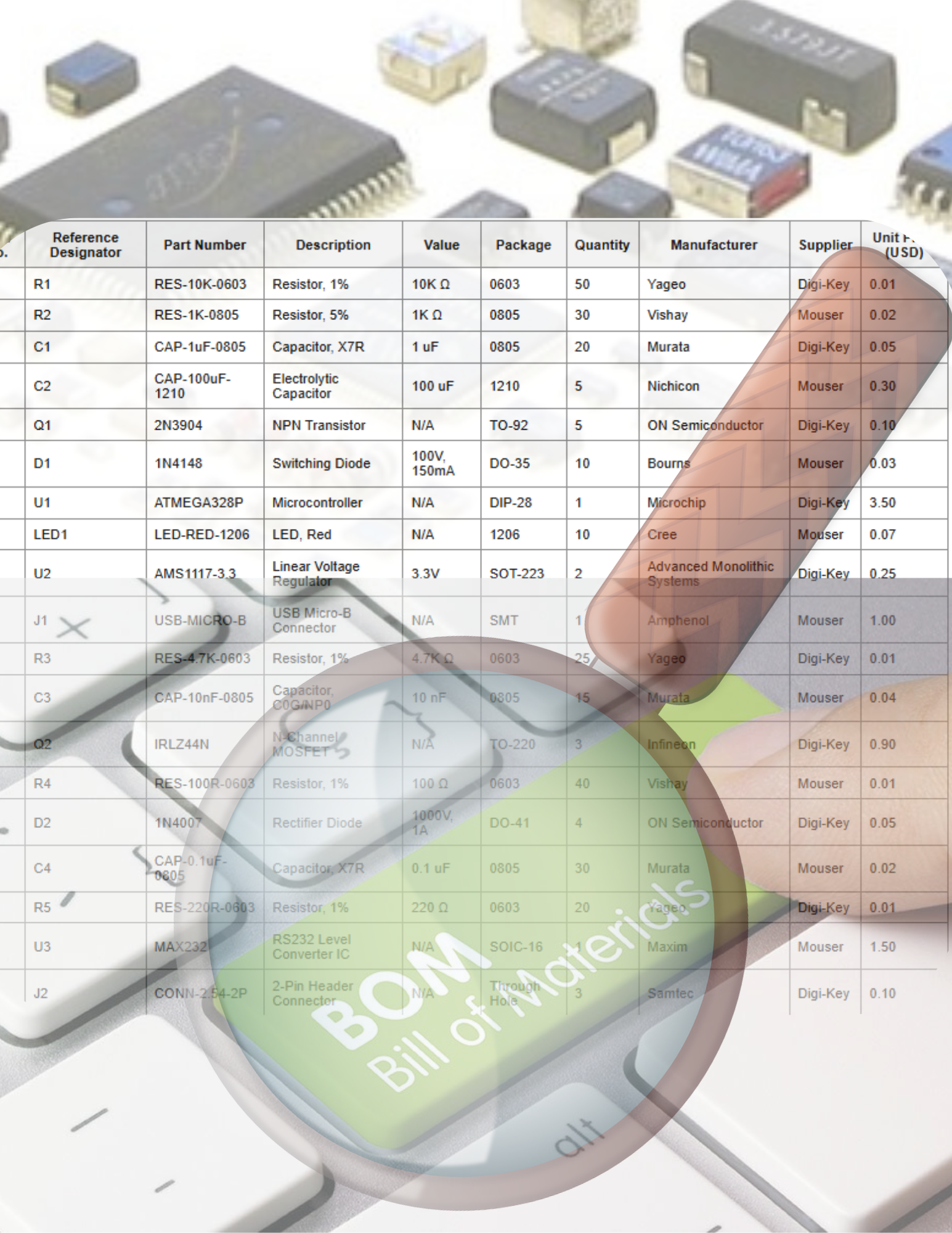
Ensure all part numbers, quantities, and specifications are accurate and complete.
Identify stock issues, long lead times, or discontinued parts early in the process.
Recommend cost-effective or readily available alternatives for unavailable parts.
Collect competitive quotes from multiple suppliers to get the best value.
Provide detailed cost analysis per unit and for full batch production.
Assess supplier minimum order quantities and estimated delivery timelines.
Evaluate lifecycle status to avoid using obsolete or near end-of-life components.
Adjust BOM pricing based on real-time market changes and trends.
Plan purchases strategically to reduce cost and prevent delays.
Return the complete data in the desired format on time
🤖 DFA (Design for Assembly) / Pick & Place Programming
We optimize layout to reduce machine travel and streamline the assembly process.
Ensure each component footprint matches its actual specifications perfectly.
Check spacing, polarity, and alignment to avoid placement or reflow issues.
Create accurate centroid (XY) files for automated pick & place machines.
Clean up silkscreen text placement for easier inspection and debugging.
Review height limits to ensure no interference during machine placement.
Classify each component by assembly type—such as SMT, THT, press-fit, or afterwash—to ensure accurate processing during production.
Deliver PnP files, BOM links, classifications, and guidelines for assembly.
Stencil Preparation
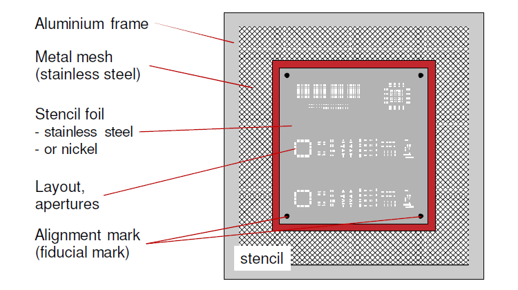
Carefully review solder paste layer files to ensure all pads are correctly represented and aligned.
Adjust aperture sizes and shapes based on pad size, component type, and assembly requirements.
Tailor aperture dimensions and paste volume for critical components like BGAs, QFNs, and fine-pitch ICs for reliable soldering.
Apply standard industry or customer-specific stencil design rules for optimal solder paste deposition.
Ensure stencil openings align perfectly with panelized PCB layouts and include fiducials if required.
Finalize stencil files with precise formatting to ensure compatibility with manufacturing processes.