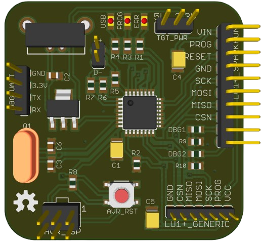
PCB Designing
Our PCB designing services ensure precision, reliability, and manufacturability from concept to production. Using advanced CAD tools, we develop optimized board layouts that meet industry standards and application-specific demands. Whether it's a simple single-layer board or a complex high-speed multi-layer design, we deliver robust and scalable designs with complete documentation and support.
Build from Concept
Schematic Capture / Layout Design
Develop clear and precise circuit diagrams with proper net naming and hierarchy.
Design optimal trace routing, layer stack-up, and placement to ensure signal integrity.
Handle impedance control, differential pair routing, and length matching for fast signals.
Apply RF layout techniques and shielding to minimize noise and interference.
Design for heat dissipation using copper pours, thermal vias, and component spacing.
Run extensive DRCs to ensure manufacturability and reliability.
Maintain accurate symbol and footprint libraries for consistency and reusability.
Deliver production-ready files including Gerber, drill, pick & place, and assembly drawings.
Generate schematic PDFs, BoM, netlists, and design reports for stakeholder review.
Track design revisions and maintain change history using version control systems.
🛠️ Tools & Industry Standards
We use Altium Designer, KiCad, OrCAD, Eagle, and other professional platforms.
All designs follow IPC standards for Class 2 and Class 3 applications.
Ensure component selection and materials meet RoHS directives and regulations.
Conduct DFM, DFA, and signal integrity reviews before production release.
Industries Served
Reverse Engineering
PCB Reverse Engineering is the process of thoroughly analyzing a printed circuit board (PCB) to reconstruct its design when original documentation—such as schematics, fabrication files, or component lists is unavailable. This detailed process involves careful examination of the board to identify components, understand their functions, and trace electrical pathways across different layers.
By studying the board’s structure systematically, engineers recreate accurate design documentation that enables continued product support, maintenance, or redesign. This is particularly critical for legacy equipment, discontinued products, or essential infrastructure where access to the original design is no longer possible.
Successful reverse engineering requires both technical precision and deep electronic expertise to ensure that the recreated design faithfully reflects the original board's function and performance. The end result is a complete design package that can be used for further development, repair, or replication.
How We Approach Reverse Engineering
We begin with a detailed visual inspection, capturing high-quality images of the board’s surfaces and identifying all visible elements.
Each component is analyzed for type, value, and purpose. Obsolete parts are flagged, and suitable replacements are proposed if necessary.
Electrical paths are traced with precision to map interconnections, including inner layers in multi-layer PCBs, ensuring all nets are accounted for.
Based on traced connections, a logical schematic is recreated to represent the functional design of the original board.
Using the schematic and board visuals, we rebuild the PCB layout while ensuring compliance with modern manufacturing standards.
A detailed parts list is created, including specifications and sourcing options for each component.
The recreated design is verified against the original board to ensure functional accuracy. Testing is performed where feasible to confirm performance.
We provide ongoing support and recommendations to enhance design robustness and facilitate future upgrades.
Note: Reverse Engineering Services Available For Up To 2 Layers Only.
Legal Acceptance
We Accept
- Reverse engineering for legacy systems maintenance
- Unsupported product design recreation
- Repair and refurbishment of critical infrastructure
- Educational and research purposes
We Don’t Accept
- Reverse engineering for intellectual property infringement
- Unauthorized duplication of proprietary designs
- Use of reverse engineering for illegal or unethical purposes
- Design recreation without proper permissions